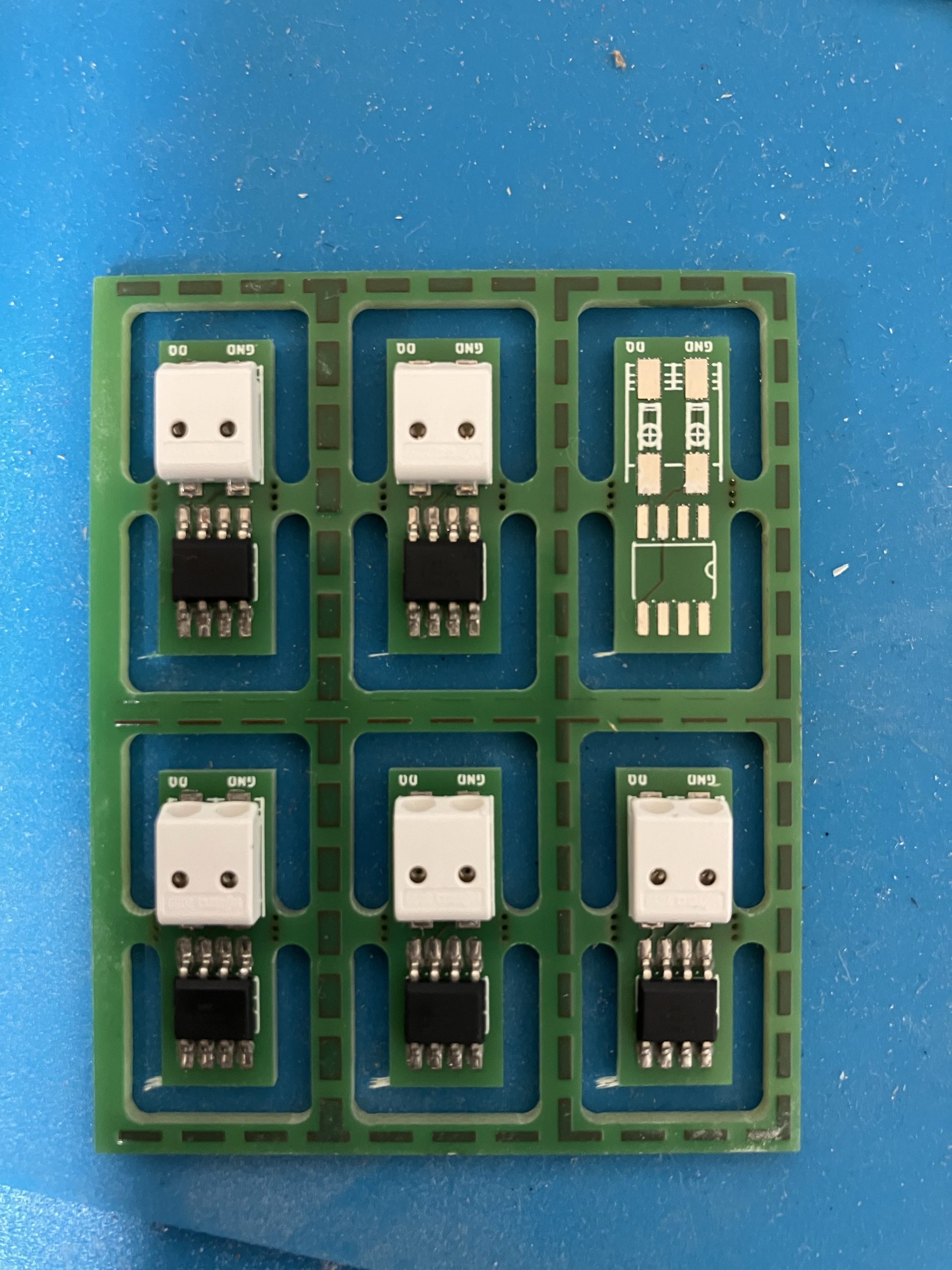
After creating the first few temperature sensors the PCB has been updated. It’s smaller now. Soldering went smoothly. The fact that the PCBs came in groups of 6 made applying the solder paste much faster. After soldering the PCBs did not look very nice. But after measuring all were as expected and the question is whether to clean the PCBs would help to make sure the the remaining dirt does not cause long term problems. Unfortunately an off by one issue appeared.
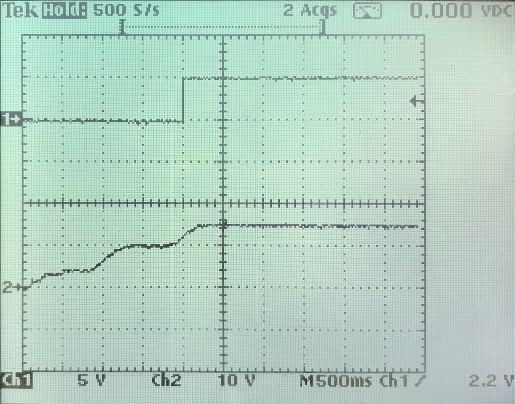
After a (luckily unsuccessful) search for short cuts I have connected the power supply part on the pcb to an external power supply. The following screen shot shows that the power supply becomes operational at around 12V.
Channel 1: Vout Channel 2: Vin (manual rise from 0 to 15V )
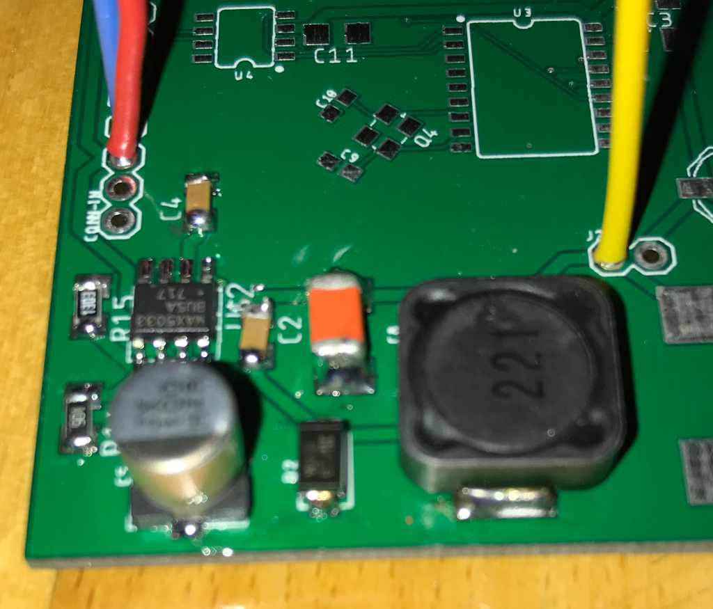
Unfortunately I do not have a nice load to check the behavior close to the 0,5A the power supply is designed for. But I have small light bulb that causes a load of around 30 mA. Running the power supply at this load for some minutes did not cause any noticeable increase of the temperature. That’s a good sign. I also tried a short cut between Vout and GND. Nothing bad happened. The MAX5033 detected the short cut and shut off, before trying to start again. After removing the short cut it went back to normal. This state I did not try for a longer time. The effects were visible on the oscilloscope and audible. Typically the inductors start to “sing” under such conditions.
My external power supply can only provide 20V, but I assume, that if everything works at 20V it’ll also run at 24V. So the next step before actually connecting the arduino is to run the power supply for an extended period of time (~ 1 day) with high load and 24V input.
After a long time I’ve reactivated my solder iron. Since I’ve done that without additional flux (apart from the content of the solder) the result looks accordingly. My next step will be testing the circuitry.
Surprisingly for me the soldering of the IC was the easiest. I assume, that the pads were perfectly sized for hand soldering. The resistors and small capacitors look horrible because I did not use tweezers. The large capacitor’s solder pads are a bit too small for hand soldering and the inductor needs a higher temperature because of the relatively high mass.
I also noticed that I’ve to improve my documentation. More information on the pcb, the layout and the circuit diagrams are required to simplify the soldering and reduce the time spent on searching the parts and their orientation. For example having the small dot that indicates pin 1 of an IC would be very helpful. Also the orientation of the larger capacitors and the exact location and size of the text on the pcb.