… but the programmers of the Withings app wanted to make sure that I’m aware that there is nothing to see.
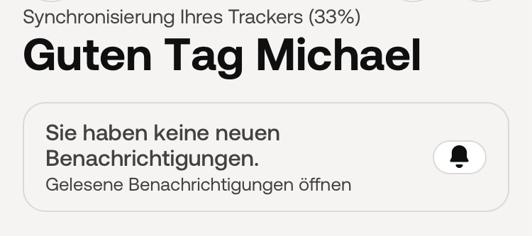
Spending one third of the screen to tell that there’s nothing new seems to be wrong.
… but the programmers of the Withings app wanted to make sure that I’m aware that there is nothing to see.
Spending one third of the screen to tell that there’s nothing new seems to be wrong.
Felix found four-leaved clover

during our hike around BioRia
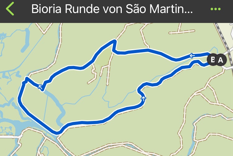
It seemed to be a local variation since it appeared multiple times within a few square meters. We even found a five-leaved.

The German school in Porto has it’s own Oktoberfest. It was fun and games for the kids and of course you meet more BOSCHlers.
I received a care package. Ingredients for the world famous “Linsen, Spätzle und Saitenwürstle”.
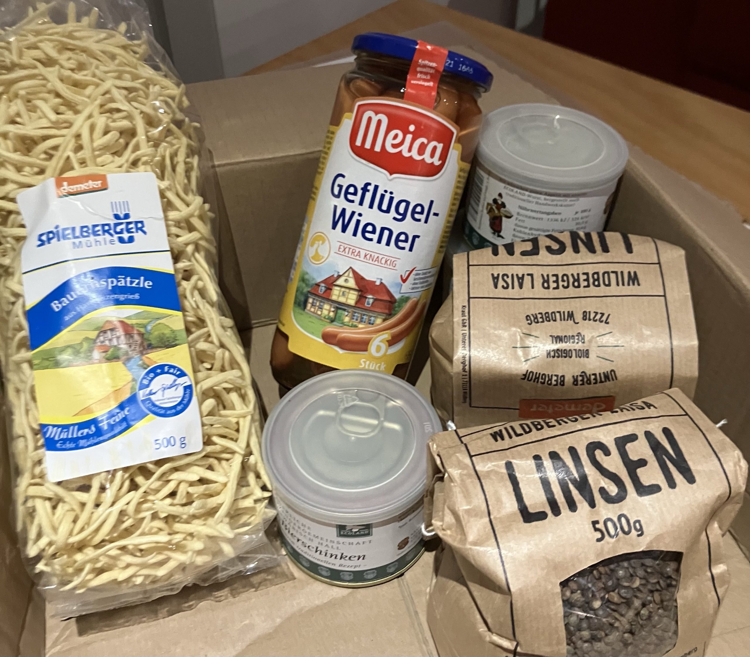
Plus canned sausage. All a Swabian needs. Except bread. Like all, or at least most, other Germans living abroad: Bread is a topic that requires some intensive investigation.
Next to our house is a heli pad. Never saw it in action before. Today I caught it.

However I’ve not yet seen it on any flight tracking site. I might have to start up the old TV usb stick.
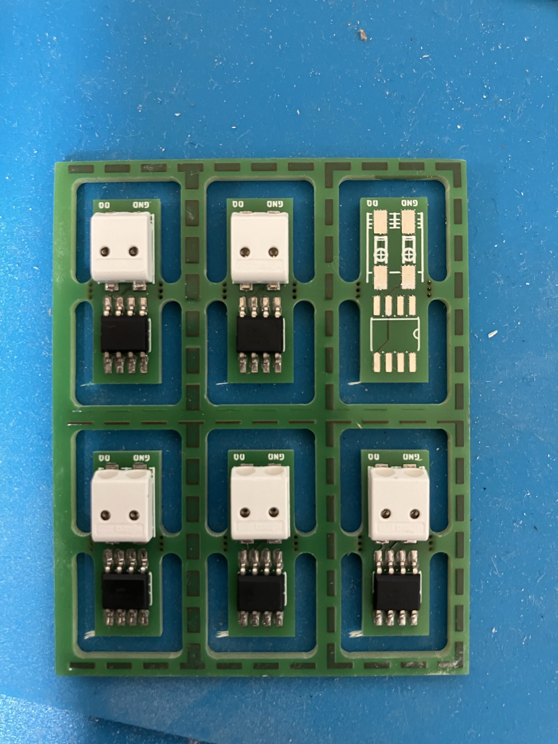
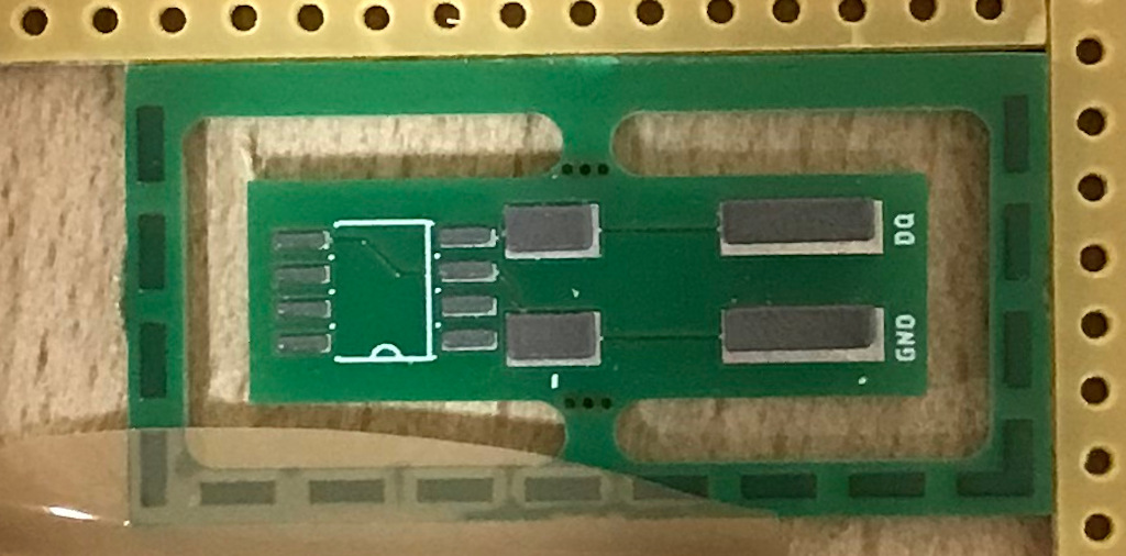
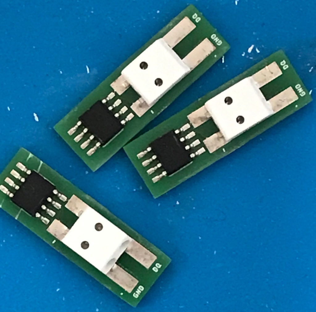
After creating the first few temperature sensors the PCB has been updated. It’s smaller now. Soldering went smoothly. The fact that the PCBs came in groups of 6 made applying the solder paste much faster. After soldering the PCBs did not look very nice. But after measuring all were as expected and the question is whether to clean the PCBs would help to make sure the the remaining dirt does not cause long term problems. Unfortunately an off by one issue appeared.
A little bit up the river from our house is the Dom Luís I bridge. Even though Eiffel’s design was rejected his former partner Théophile_Seyrig was awarded with the project. So the similarity is not purely accidential.
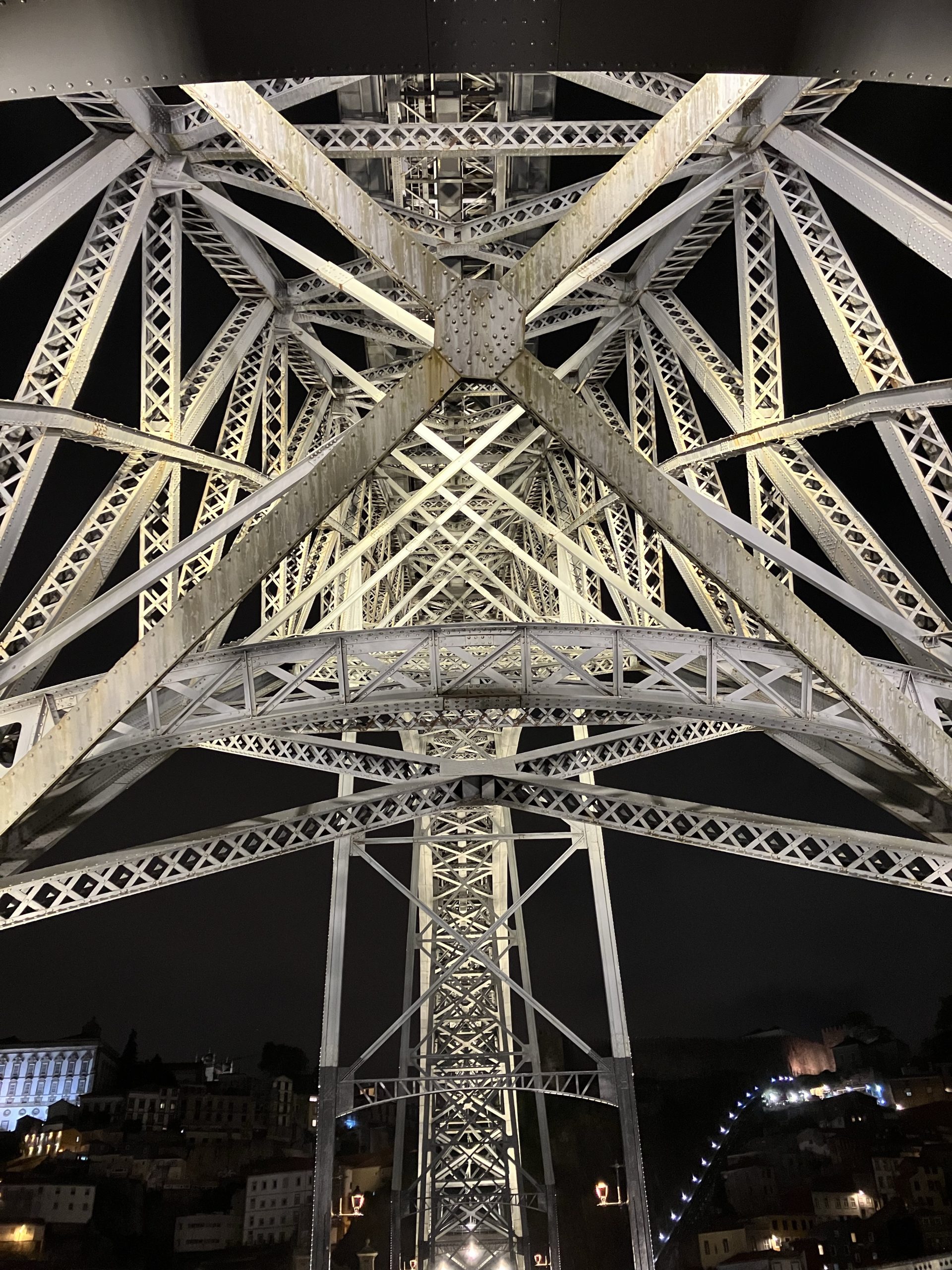
Is it a fisherman’s net or art or as my Ninjago-fluent son suggests: spinjitzu

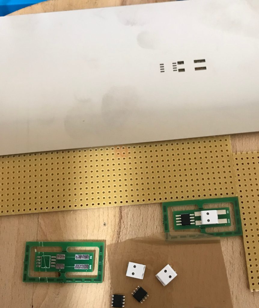
Before I proceed to manufacture the PCBs for the home automation I decided to invest in a solder plate and try a very small project: Temperature sensors that consists of a DS18B20 1-wire temperature sensor and a 2-pin SMD push connector.
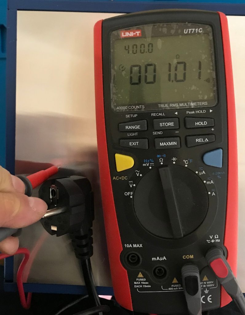
First step was to make sure that the solder plate is actually grounded properly.
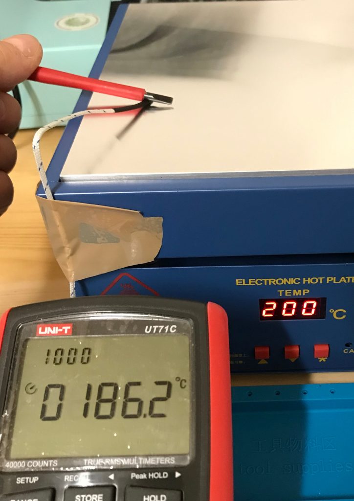
After that a layman’s temperature calibration run. Comparing the temperature using my multi-meter’s temperature probe and the internally measured value of the solder plate.
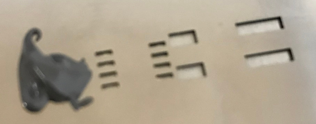
The PCBs were designed with eagle and manufactured by AISLER. They look good, were reasonably priced and came with a stencil.
On to solder paste application. The setup consists of a piece of wood with two pieces of PCB with the same thickness as the target PCB and the stencil taped in place after alignment. You can see in the image that the stencil is far from perfectly parallel to the hole line. The effect of slightly offsetting the solder paste will be visible soon.
Flipped the stencil over and put a drop of solder paste.
Using a metal scraper to apply.
The above mentioned error is visible, but I hope that it does not cause issues later and the amount of solder paste looks good. Next step is placing the parts.
Now let’s heat it up. Since I’m using the solder plate for the first time I did not take enough pictures to capture the whole reflow solder profile. I’ve set the temperatures manually and have waited using a timer. The relatively slow solder plate ensures the ramping is not too fast. The cooling after reaching maximum heat is a little bit slow, but will be improved once I’ve the ventilation in place that is definitely required for larger projects. The fan is already in place, so I’ll have to add an enclosure only.
Wait until it’s cooled.
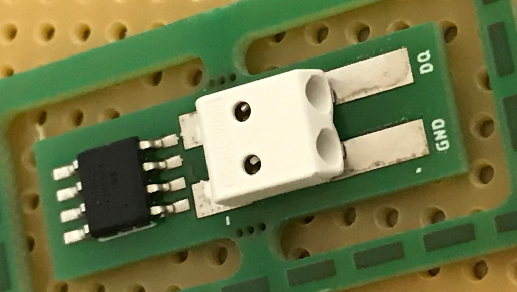
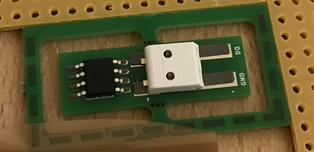
Considering the fact that the connector does not match 100% with the footprint (the 8D process will show what went wrong) the solder joint is acceptable. The temperature sensor looks good to me. (Feedback welcome). After the first one was successful I finished the series by soldering the remaining 2 parts.
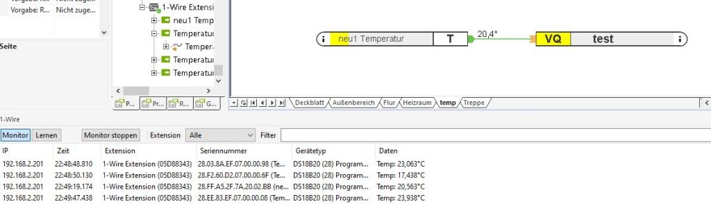
PCBs routed and sanded. I did a quick electrical test. With only 2 connections it could easily be done with the multi-meter. So the next step was to integrate the new sensor in the existing Loxone home automation system.
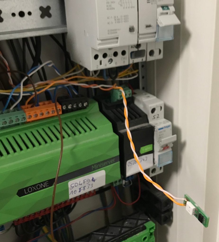
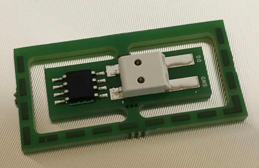
The sensor was successfully detected and provided a reasonable temperature.
In addition I’ve placed one of the sensors outside and it also show values that made sense.
I’ll order more PCBs and run a second batch and after that I’ll be out of excuses for producing the bigger PCBs for my light switches.
I’ve connected the Arduino pro mini (328/5V) to my pcb. Of course it’s not directly soldered to the PCB but using a connector, so I can replace the parts that get bricked during development. I’ve downloaded the blink example using something like this. Directly after flashing it worked, but once I disconnected the flashing adapter it stopped. After remembering, that I’ve to short my optional filter in case it’s not assemble it works.